

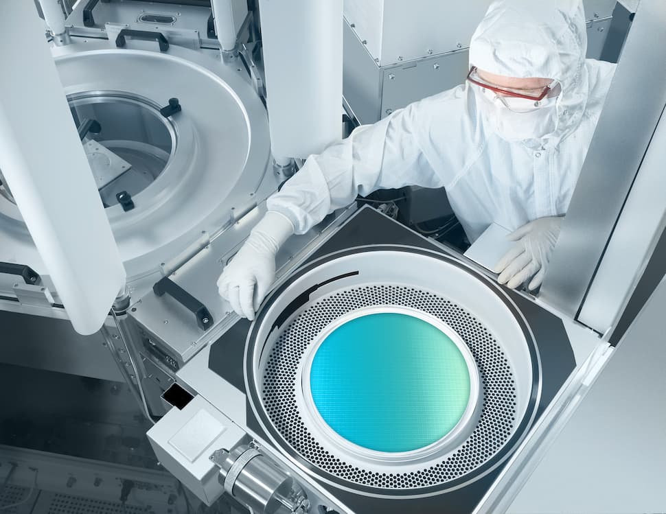
Notably, two of the largest chip equipment makers in the world are spending billions right now, and neither is building a factory. Applied Materials committed roughly $5 billion to a single research campus in Silicon Valley. Meanwhile, Lam Research committed more than $3 billion to expand labs across three continents. In effect, semiconductor equipment R&D has become its own competitive arena, separate from the fab buildout it serves.
Lam Broke Ground in Oregon
Lam Research announced the $3 billion program on August 13, 2026. Subsequently, it broke ground on the first major piece in Tualatin, Oregon on August 26. Specifically, the 120,000 square foot facility opens in 2028. Once complete, it will expand cleanroom lab space at the company’s Tualatin research center by more than 50 percent.
The stated goal is throughput of experiments rather than square footage. Lam says the program will increase experiment capacity by more than 50 percent over five years. Specifically, the work targets deposition and etch process development, materials science, and hardware validation.
This expansion reflects our continuing commitment to advancing the Silicon Forest as a leader in U.S. semiconductor innovation.
Sesha Varadarajan, Executive Vice President and Chief Operating Officer, Lam Research
Lam expects roughly 900 construction jobs over three years and more than 400 new company positions at completion. Consequently, its Oregon headcount would rise above 11,000. Additionally, the company projects about $500 million in economic output during construction and $1.8 billion a year afterward. Additionally, Governor Tina Kotek and Senator Jeff Merkley both spoke at the groundbreaking, as did an executive from Intel.
Applied Materials Took the Opposite Approach
By contrast, Applied Materials concentrated its semiconductor equipment R&D in one very large room instead of several distributed ones. Details of the program are on the company’s EPIC Center page. Its EPIC Center in Silicon Valley represents roughly $5 billion, the largest commitment to advanced semiconductor equipment research in United States history. Moreover, Applied positions it as the nexus of more than $25 billion in research investment over its first decade.
The structural difference is who else gets in the building. Applied has recruited outside partners into EPIC. Specifically, Samsung Electronics joined on the manufacturing side, alongside Arizona State University, Rensselaer Polytechnic Institute, Stanford, and UC Berkeley on the academic side. That is a consortium model, and it trades some control for shared cost and a wider talent funnel.
| Element | Lam Research | Applied Materials |
|---|---|---|
| Committed spend | More than $3 billion over 5 years | Roughly $5 billion |
| Structure | Distributed global lab network | Single Silicon Valley campus |
| Stated metric | Experiment capacity up more than 50% | Nexus of $25B+ R&D over 10 years |
| Outside partners | Customer collaboration, Intel nearby | Samsung, ASU, RPI, Stanford, UC Berkeley |
| Timing | Oregon lab opens 2028 | Operational 2026 |
Why Semiconductor Equipment R&D Became the Constraint
Deposition and etch are the steps where atomic-scale structures actually get built, layer by layer. Device architectures then moved vertical, with 3D NAND stacking layers and logic shifting to gate-all-around transistors. As a result, process steps per wafer climbed while the tolerance for error narrowed.
Developing those processes is empirical work. An engineer runs an experiment on real hardware with real wafers, measures the result, adjusts, and runs it again. No simulation shortcut removes the need for chamber time. Consequently, the rate of progress depends on how many experiments a company can physically run.
Furthermore, the customers set the clock. When leading chipmakers compress their own node transitions to meet AI demand, the toolmaker must have qualified processes ready in advance. Lam’s chief executive, Tim Archer, framed the situation bluntly in describing the pace of innovation as relentless.
The Silicon Forest Cluster Effect
Lam’s choice of Tualatin is not incidental. Oregon’s Silicon Forest concentrates chipmakers, toolmakers, and a technician workforce in a compact geography. Furthermore, Intel is both Lam’s neighbor there and its customer. Proximity matters more than usual in this business, because process development requires engineers from the tool vendor and the chipmaker working on the same hardware.
Applied made a parallel bet on a different cluster. Silicon Valley offers university density and venture-adjacent talent that Oregon does not, while Oregon offers customer adjacency and manufacturing depth that the Bay Area has largely lost. Both are defensible reads of where the bottleneck sits.
What It Means for Suppliers
An advanced research cleanroom is among the most demanding industrial buildings that gets constructed. Vibration isolation, air handling, ultrapure water, specialty gas distribution, and exhaust abatement all run to specifications tighter than a conventional plant. Notably, they often run tighter than a production fab, because experiments are more sensitive than a stabilized process.
Accordingly, the bid packages skew toward specialized mechanical, electrical, and process-utility contractors rather than general industrial builders. The Oregon project alone carries roughly 900 construction jobs across three years, and Applied’s campus has been drawing similar trades in California. For firms already qualified on fab work, research facilities are adjacent and the qualification largely transfers.
Frequently Asked Questions
How much is Lam Research investing in R&D labs?
Lam announced more than $3 billion over five years on August 13, 2026 to expand its global lab network and increase experiment capacity by more than 50 percent. The first major project is a 120,000 square foot lab in Tualatin, Oregon that opens in 2028.
How does Applied Materials’ EPIC Center compare?
EPIC represents roughly $5 billion in a single Silicon Valley campus and is described as the largest commitment to advanced semiconductor equipment research in US history. Applied positions it as the nexus of more than $25 billion in research investment over its first ten years.
Why are chip equipment makers building labs instead of factories?
Process development for deposition and etch is empirical and requires chamber time on real hardware with real wafers. Progress is limited by how many experiments a company can run, so lab capacity rather than production capacity is the binding constraint.
What is the Silicon Forest?
The Silicon Forest is the semiconductor cluster in the Portland, Oregon metropolitan area, including Hillsboro and Tualatin. It concentrates chipmakers such as Intel alongside equipment suppliers and a specialized technician workforce.
How many jobs will the Lam Research Oregon lab create?
Lam expects roughly 900 construction jobs over three years and more than 400 new company positions at completion, bringing its Oregon total above 11,000. The company projects $500 million in economic output during construction.
What do deposition and etch actually do?
Deposition adds material layers onto a wafer and etch selectively removes material to form structures. Together they build the atomic-scale features of a chip, and both grew more demanding as devices moved to 3D NAND stacking and gate-all-around transistors.
The Bottom Line
Semiconductor equipment R&D spending of this size signals that the industry expects the pace of node transitions to hold, and the toolmakers intend to be ready before their customers ask. For related coverage see US solar wafer manufacturing, the full IndustrialSage Headlines Ep. 32 breakdown, our reporting on Hanmi Semiconductor’s US expansion, or the US Manufacturing Investment Tracker.

Author: Wes Garrett
Content and Growth Marketing Producer | From Strategy to Execution, Delivering Impactful Media Solutions and Client Success


