

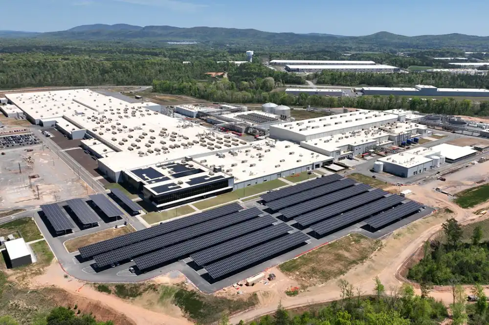
A silicon ingot produced in the United States frequently travels overseas for slicing into wafers, then comes back to become a solar cell. That round trip describes exactly what American solar manufacturing lacks. Moreover, it is the gap Tesla’s proposed $10.1 billion Texas plant would target.
Where US Solar Wafer Manufacturing Actually Stands
American solar module assembly grew explosively, expanding more than 750 percent in a few years to reach roughly 70 gigawatts of capacity. Walk into one of those plants and the work looks like real manufacturing, because it is. The cells going into those modules, however, mostly are not American.
US solar wafer manufacturing capacity sits at about 5 gigawatts against actual production near 3.2 gigawatts. Those figures come from PV Tech’s analysis of US supply chain bottlenecks. That covers less than 63 percent of the crystalline cell segment it feeds. Active ingot and wafer capacity comes from just two operators, Hanwha Qcells and Corning, totaling roughly 5.3 gigawatts.
The step above is not the constraint. Domestic polysilicon production from Hemlock Semiconductor and Wacker Chemie holds around 40,000 metric tons, enough to supply approximately 21 gigawatts of solar production. Consequently, existing wafer capacity uses only about 20 percent of the polysilicon capacity sitting above it.
| Supply chain step | US capacity | Producers |
|---|---|---|
| Polysilicon | ~40,000 metric tons, supports ~21 GW | Hemlock Semiconductor, Wacker Chemie |
| Ingot and wafer | ~5.3 GW capacity, ~3.2 GW production | Hanwha Qcells, Corning |
| Module assembly | ~70 GW | Many |
What an Ingot Is, and Why the Step Matters
Polysilicon arrives as chunks of refined silicon. Growing an ingot means melting that silicon and pulling a single large crystal from the melt. Typically that uses the Czochralski method, which produces a cylindrical block. That block then gets sliced into wafers a fraction of a millimeter thick, and those wafers become cells.
Ingot growth and wafering are the capital-intensive, energy-intensive, precision-heavy steps. They are also where China concentrated its advantage. Skipping them domestically means the finished module carries an American label while its most technically demanding component crossed an ocean twice.
What Tesla Filed
A tax incentive application submitted under the codename Project Crystal Sun describes a $10.1 billion solar cell plant. Specifically, it covers roughly 3,050 acres in Fort Bend County, near Richmond and southwest of Houston. The filing splits the spend into about $1.5 billion of real property and $8.6 billion of equipment across 2026 through 2028. Furthermore, it projects commercial production in the first quarter of 2029 and 9,712 permanent jobs at full build.
The equipment-heavy ratio is itself informative. Roughly 85 percent of the capital goes to tooling rather than buildings, which is what ingot growth and wafering economics look like. Module assembly lines do not carry that ratio.
The status deserves emphasis. Tesla is asking Fort Bend County for property tax relief to make Texas competitive, and the company says it is still weighing sites in other states. Neither Tesla nor the county has said when a decision comes, so the filing is a real public document describing a project that remains a proposal.
US Solar Wafer Manufacturing Has an Announced-Versus-Operational Problem
Solar manufacturing has a credibility gap that any reader should apply to this filing. Roughly $43.1 billion in US solar manufacturing investment had been announced against only about $14.5 billion operational by mid-2026. Announcements in this sector convert to running lines at a meaningfully lower rate than in, say, food or automotive.
At least 21 gigawatts of domestic wafer capacity has been planned on paper, unlocked in part by federal incentives, and the SEIA supply chain dashboard tracks what has actually come online. Actually building it is the harder half.
The Incentive Timing Is Awkward
Section 45X advanced manufacturing credits provide meaningful support, including roughly $0.07 per watt for domestically assembled modules. Furthermore, the program extends production credits to domestic wafer facilities. Here the calendar works against the buildout.
Clean Energy Associates puts the realistic timeframe for new wafer facilities at 2029 to 2030, which is precisely when the 45X credit begins to taper. A developer sizing a wafer plant today is therefore modeling a facility that reaches volume production as its principal subsidy declines. Tesla’s own filing targets first quarter 2029 production, placing it inside that same window.
Trade policy offers only partial help. Analysts have described Section 232 as offering limited prospects for US wafer capacity. Specifically, tariffs raise the cost of imported wafers without addressing the capital intensity, energy cost, and technical depth that make the step hard to localize.
Why Industrial Readers Should Track This
Wafer and ingot plants are not light industrial facilities. They demand large, stable electrical loads, ultrapure process utilities, precision handling and inspection, and cleanroom discipline that overlaps substantially with semiconductor fabrication. In practice, the vendor base is closer to the chip industry than to conventional panel assembly. Accordingly, the step has been slow to localize.
That overlap also cuts the other way. Firms already qualified for semiconductor process equipment, ultrapure water, specialty gases, and cleanroom construction are the natural bidders. That holds whether a plant of this scale lands in Texas or anywhere else. The same equipment-intensive dynamic is reshaping chip toolmakers, which we cover in our reporting on AI chip equipment suppliers entering the US market.
Frequently Asked Questions
How much solar wafer capacity does the US actually have?
US wafer capacity is roughly 5 gigawatts with production near 3.2 gigawatts, supplied by Hanwha Qcells and Corning at about 5.3 gigawatts of combined ingot and wafer capacity. That covers less than 63 percent of the crystalline cell segment it feeds.
What is a silicon ingot in solar manufacturing?
An ingot is a single large crystal of silicon pulled from molten refined silicon, usually by the Czochralski method. It is then sliced into wafers a fraction of a millimeter thick, and those wafers are processed into solar cells.
Why does the US import wafers if it produces polysilicon?
Domestic polysilicon capacity of about 40,000 metric tons could supply roughly 21 gigawatts of production, but wafer capacity uses only about 20 percent of it. Because wafering capacity is so limited, US-produced ingots are often shipped abroad for slicing and returned for cell processing.
Has Tesla committed to building the Texas solar plant?
No. Tesla filed a tax incentive application for a $10.1 billion plant in Fort Bend County and is seeking property tax relief, but says it is still weighing sites in other states. No decision timeline has been announced.
What does ingot to module under one roof mean?
It means performing every step from crystal growth through finished panel assembly at a single site: ingot growth, wafering, cell processing, and module assembly. Most US solar manufacturing performs only the final step using imported cells.
How does the 45X credit affect solar wafer plants?
Section 45X provides advanced manufacturing production credits, including roughly $0.07 per watt for domestic modules, and extends credits to wafer facilities. Clean Energy Associates places new wafer plants at 2029 to 2030, which coincides with the credit beginning to taper.
The Bottom Line
US solar wafer manufacturing is the step that decides whether a domestic panel is genuinely domestic, and one filing in Fort Bend County will not settle it. See the full IndustrialSage Headlines Ep. 32 breakdown, our US Manufacturing Investment Tracker, or more manufacturing and industrial news.

Author: Wes Garrett
Content and Growth Marketing Producer | From Strategy to Execution, Delivering Impactful Media Solutions and Client Success


